New technologies and familiar challenges could make semiconductor supply chains more fragile
With escalating trade restrictions on critical next-gen AI chip technologies, leaders should adapt quickly to make supply chains more resilient
Geopolitical tensions and escalating trade restrictions are reshaping semiconductor supply chains, with far-reaching impacts for artificial intelligence chip innovation, the global economy, national security, and scientific progress. Many of these high-tech processes and materials rely on a handful of suppliers, whose dominance in key regions has prompted governments to impose trade barriers to protect strategic interests and reduce dependency. Making the world’s most advanced chips for next-generation AI systems and high-performance computing data centers has, for a long time, meant navigating fragile supply chains, but the stakes are much higher now.
Deloitte expects that, by 2026, semiconductor technologies, including front-end and back-end chip manufacturing such as etching and gate-all-around (GAA) transistors, electronic design automation (EDA), and software tools that enable advanced AI models, will become additional supply chain chokepoints. And Deloitte predicts that, in 2026, at least US$30 billion will be spent on various critical technologies, including extreme ultraviolet (EUV) lithography equipment and high-bandwidth memory co-packaging tools, which will be affected by trade barriers.1 However, this investment will be dwarfed by the approximately US$300 billion AI chips market that these technologies will enable, underscoring the critical role in the global semiconductor supply chain.2
AI (re)writes and (re)shapes global semiconductor supply chains
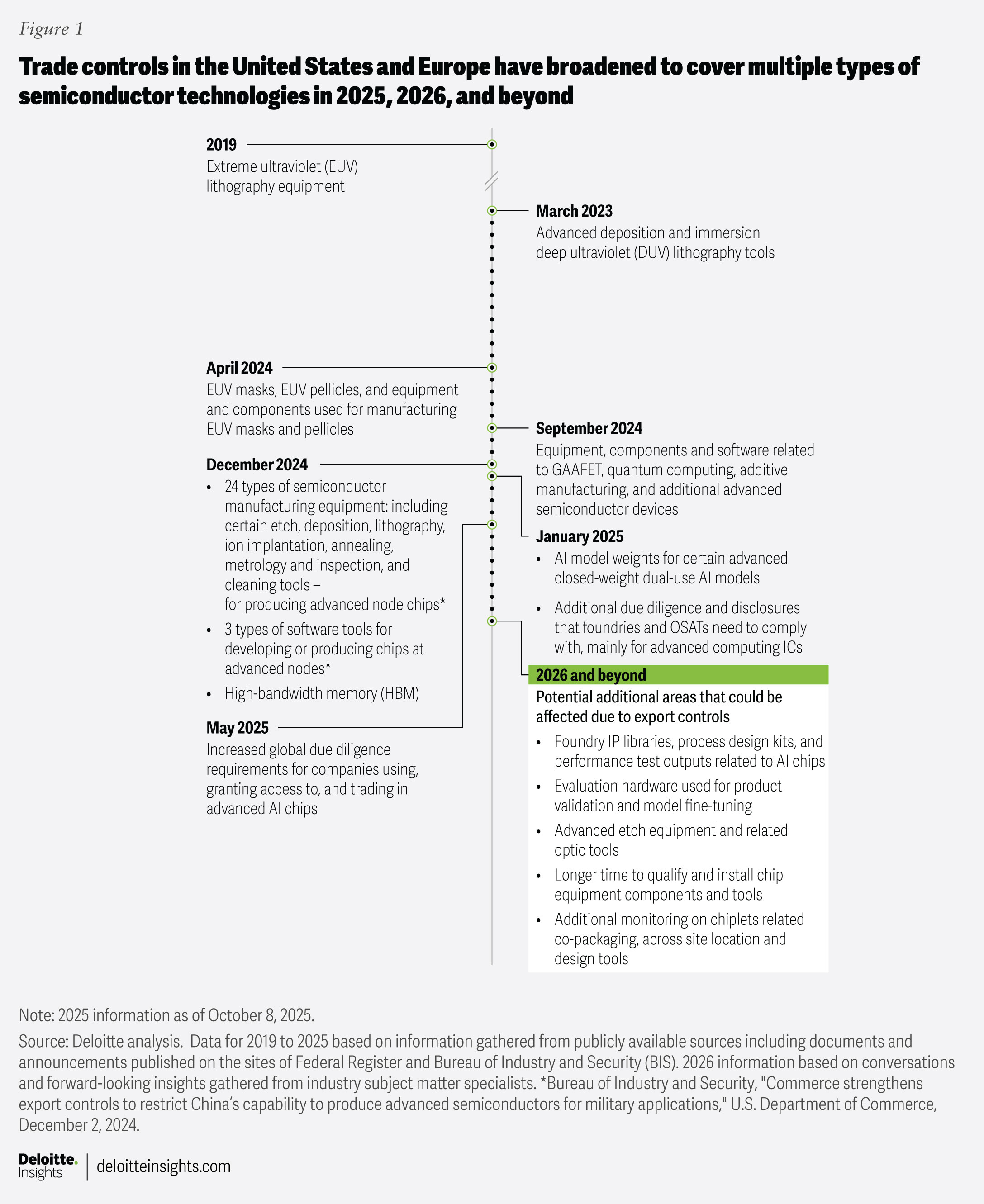
Deloitte’s analysis of semiconductor content in AI data centers noted that the global semiconductor supply chain is deeply interdependent, and countries are working to protect their access to AI chips and hardware components that are critical for generative AI, high-performance computing, and autonomous systems.3 Therefore, it’s not surprising that export controls and other trade restrictions have started to affect a broader footprint of semiconductor equipment, materials, software, design tools, various kinds of chips, and packaging and assembly tools in 2025 and 2026 compared to two or three years ago (figure 1).
An AI system’s performance depends on a narrow stack of several globally distributed technologies, including advanced AI logic design, leading-edge front-end node fabrication, and advanced packaging. Delivering these capabilities involves collaboration among multiple stakeholders, such as integrated device manufacturers, foundries, equipment makers, design vendors, outsourced semiconductor assembly and test (OSAT) vendors, system integrators, outsourced channel distribution partners, and government bodies from different countries.4
Export controls redefine the future of advanced AI logic design
In 2024 and 2025, US restrictions tightened and then eased on multiple critical semiconductor technologies, especially EDA tools.5 EDA processes constitute the design logic, chip layout and placement, simulation, AI-enhanced design, verification, and integration workflows, all of which are vital for developing advanced AI accelerators.
As an example, there was an existing restriction for chips developed based on gate-all-around field-effect transistor (GAAFET).6 GAAFET is an emerging transistor architecture for sub-5 nm and sub-3 nm logic design, offering performance and power efficiency benefits for compute-intensive gen AI workloads. In December 2024, the United States further broadened export controls to include software and tools that support the development and design of advanced computing nodes.7 As these new export controls emerge, they are likely to have implications for the broader EDA ecosystem and foundry partners in 2026.
Prediction and perspectives for 2026 and beyond
As restrictions on GAAFET-based chips increase, foundries in non-US allied countries using GAAFET process design kits for leading nodes will require EDA tool support for validation. But if a region lacks access to these tools, it may have to rely on older, less efficient nodes, or be pushed toward developing domestic EDA capabilities, both of which will likely stretch product cycles and dent competitiveness. Moreover, added controls on advanced computing chips and new controls on AI model weights have increased compliance requirements for companies collaborating with customers and business partners, especially in China.8 Increasingly, AI models and the scale and quality of AI model weights are influencing the capabilities of AI-powered EDA tools that are used to design chips.9
By 2026, Deloitte predicts that EDA and logic design players will likely be impacted by these controls: They could face more intense checks and granular disclosure requirements regarding entity, location, and end use of foundry intellectual property libraries, process design kits, and performance test outputs tied to AI accelerators. Evaluation hardware, typically used for product validation and model fine-tuning (including reference model weights for testing purposes and outputs), may come under closer scrutiny.10 Companies involved in AI hardware co-design may need to establish trusted country pathways or may have to retool workflows: For example, they could keep model weights within the United States or an ally’s secure IT infrastructure while allowing foundry partners to run tests remotely.11
Chokepoints in developing leading-edge front-end node fabrication for AI systems
The United States and the Netherlands continue to restrict access to EUV equipment, which is widely regarded as essential for producing the most advanced process nodes.12 While the United States does not have domestic EUV production capabilities, it influences which countries can buy these machines by coordinating export restrictions with allies (such as the Netherlands), mainly to secure technological and national security. At the same time, China has pushed forward to develop lithography equipment by customizing deep ultraviolet technology using multiple patterning techniques through its domestic chip equipment companies.13 While these methods appear effective, they operate at much slower speeds and higher costs.14 To safeguard national security interests, the United States introduced additional export restrictions on tools used for precision etching that are essential to carve intricate AI architectures.15
Prediction and perspectives for 2026 and beyond
Advanced etch technology is critical for fabricating leading-edge AI chips at sub-5 nm nodes. The chip industry employs double, quadruple, and spacer-based patterning to manufacture delicate features on the most modern AI chips.16 As a result, the US-originated process equipment for etching, as well as etching equipment and tools designed or manufactured abroad using the United States’ etch tech IP, could emerge as new chokepoints in 2026. In addition, components such as optics (lenses and mirrors) and reticles (photomasks), which are integral to wafer fabrication equipment and hold the blueprint of the pattern to be printed on a wafer, may also attract restrictions.
Furthermore, specialty gases (such as silane and fluorinated derivatives)17 and critical minerals (including gallium, germanium, and antimony)18 that are part of the advanced node manufacturing process introduce additional friction points in the global chip supply chains.
With a broad range of front-end process equipment, components, and input materials facing export controls, Deloitte predicts that sub-5 nm and sub-3 nm production ramps would continue to accelerate in the United States, Taiwan, and South Korea through 2026 and beyond. Meanwhile, China is expected to continue focusing on mature deep ultraviolet technology with multiple-patterning workarounds.
Consequently, multinational chip equipment companies should adjust their front-end wafer fabrication–related capital expenditure planning at the regional level. Fabrication equipment vendors, components and parts suppliers, and foundries may face longer qualification, upgrade, and installation cycles compared to those experienced in 2024 and 2025. And as chip design companies adapt to the new requirements—developing de-featured or stepped-down AI XPUs (reduced performance versions of high-end AI chips) and region-centric process libraries to meet the growing gen AI chip demand in China and other non-US–allied countries—the need for enhanced support from front-end fabrication equipment providers will likely also rise.
Trade controls disrupt advanced packaging and testing
Advanced packaging technologies have quickly become strategic targets for export controls. Measuring and inspection equipment is facing export restrictions from the Netherlands 19 due to its critical role in high-density chip stacking,20 an essential building block for current and future gen AI chips.21 Specific types of chip equipment (etch, deposition, lithography, ion implantation, annealing, metrology and inspection, and cleaning tools) that are essential for testing and validating advanced AI chips are under export control.22 This is because they’re considered sensitive and potential dual-use technologies, and they may continue to attract additional trade controls in the future.
Prediction and perspectives for 2026 and beyond
As highlighted in the 2024 TMT Predictions, chiplets and heterogeneous architectures are fast emerging as preferred packaging models for gen AI chips designed for high-performance computing AI workloads.23 However, the complexity involved in sourcing and packaging multiple dies and components from diverse vendors from different regions will likely make chiplets a major geopolitical chokepoint in 2026. Notably, chiplet-based solutions are estimated to be worth approximately US$100 billion to US$110 billion in annual revenues in 2026.24
High-bandwidth memory (HBM) has also become crucial for gen AI training and inference workloads. As of mid-2025, HBM co-packaging was being monitored more closely, including the identification of locations where HBM and logic are co-packaged.25 As a result, semiconductor players involved in assembly, testing, and packaging will likely be required to provide additional disclosures. These may include naming the OSAT providers or back-end manufacturing vendors involved in packaging, specifying the location where the system is co-packaged, indicating the destination country where the interim or finished product is shipped to, and detailing relevant performance thresholds.
What is likely to become more prominent in 2026 and beyond is the growing dependence on the effectiveness of the back-end process to ensure new products reach the market on time. As routing and documentation requirements grow increasingly stringent for co-packaging sites—particularly those involving HBM, logic, and high-speed input/output—every aspect of the supply chain, from front-end wafer fab schedules and design sign-offs for EDA vendors to product launches by end-customer original design manufacturers and original equipment manufacturers, will become more dependent on the pace at which advanced packaging-related process clearances and procedures are completed. Any delays on the packaging vendor or the OSAT’s side could affect yield ramps and tuning, in turn, triggering re-shoring or friend-shoring by relocating facilities to allied countries.
Collectively, these factors could impact the rollout of AI data centers planned for 2026 (and beyond) across multiple regions. Hyperscalers, cloud providers, and companies across industries combined are expected to spend roughly US$500 billion in 2026 and US$1 trillion in 2028 on AI data centers,26 with chip solutions accounting for roughly 50% to 60% of that spending. Given the anticipated growth, supply chain disruptions could affect tens or even hundreds of billions of dollars’ worth of semiconductors over this three-year period.
The bottom line
China bolsters its domestic semiconductor ecosystem
Stringent export controls and restrictions on a range of semiconductor technologies have inhibited China’s access to state-of-the-art AI chips. This has prompted China to accelerate domestic semiconductor innovation, especially as it sees the moves could hamper its progress toward sub-7 nm and sub-5 nm, even as non-China chip fabs move from 3 nm and 2 nm in 2025 to 1.8 nm in 2026 and 2027.27
As China develops workarounds to deal with export controls, it may explore multiple facets of the global semiconductor supply chain, not just front-end manufacturing but also chip design and advanced packaging.28 While sophisticated chips using older manufacturing nodes can be used for advanced packaging, the United States is likely to implement additional controls and checks to limit the performance of such packaged systems meant for leading-edge AI chips.
Race to build sovereign tech stacks accelerates, ushering new regional equations
Technology sovereignty is aspirational as countries aim to independently develop, control, and regulate digital technologies.29 Since AI is widely viewed as the next major driver of economic development and national competitiveness, its ecosystem is receiving attention as governments seek greater direct control over its digital infrastructure. Countries and regions do not want to be left further behind or involuntarily forfeit their authority. This urgency is heightened because advanced AI capabilities are currently concentrated among a few countries and companies. Moreover, as both the United States and Europe are reshoring high-end chip manufacturing, they are likely to invest in alternative advanced assembly and test hubs through 2026 and beyond, domestically as well as in countries such as India, Vietnam, and Malaysia.30
Need for the semiconductor industry to bolster supply chain resilience
Chip companies across the ecosystem may need to proactively prioritize resilience through internal stress-testing exercises, primarily to self-assess their end-to-end supply chains and bolster cybersecurity preparedness.31
Robust supply-chain diversification across regions and investment in alternate sourcing strategies and channel partnerships are crucial. The strategic importance of securing independent supply chains for critical materials and components requires accelerated localization and regulatory adaptability. Moreover, geopolitical issues could fragment global AI ecosystems, presenting risks such as exporting chips through gray markets and intensifying pressures on companies to bolster product and supply chain monitoring and tracking capabilities.
Though the market for AI inference-optimized chips is expected to grow to billions of dollars in 2026, most of the advanced computing will be performed on leading-edge AI chips that would mainly reside in hyperscale data centers or at on-prem servers that use the same chips and racks as data centers do.32 Therefore, new and additional export controls and requirements could possibly be directed at AI inference chips and related infrastructure, for which the broader semiconductor industry should develop alternate supply chain options across sourcing to distribution.
And with the shift from training to inference, software’s importance as a more integral part of semiconductors will also grow, for instance, using software programming techniques to reconfigure one large monolithic AI GPU (meant for training) into multiple smaller GPU slices or virtual GPU instances (usable for inference).33
Additionally, US- and Europe-based device original equipment manufacturers may need to shift production and assembly away from China and toward the emerging hubs in Southeast Asia and India. This shift could increase costs in the short term, potentially driving consumer tech device inflation. Semiconductor companies should remain agile and operate at scale, anticipate and adapt to evolving trade patterns beyond 2026, and explore alternate strategic country-level alliances to safeguard critical logistics routes and infrastructures.
As trade tensions reshape global alliances and channel partnerships, the chip industry’s resilience faces an unprecedented test heading into 2026. The interconnected and highly strategic nature of global chip supply chains highlights the urgent need for proactive engagement and collaboration among multiple industry stakeholders to make the semiconductor supply chain more resilient.
by
Karthik Ramachandran
Duncan Stewart
Jeroen Kusters
Deb Bhattacharjee
Girija Krishnamurthy
The authors would like to thank Nina Zhang, Amy Scimeca, Karan Aggarwal, Jesse Singh, Michael Greco, and Pablo LeCour for their contributions to this article.
Cover image by: Jaime Austin; Adobe Stock
Visit the Deloitte Center for Technology, Media & Telecommunications
Access more insights for the technology, media, and entertainment; semiconductor; telecommunication; and sports sectors.